University of Cincinnati Facilities
UC has state-of-the-art facilities in the colleges of engineering, arts and sciences, and medicine to conduct the ERC projects.
Bio-Nanotechnology Labs, Tissue Engineering and Biomechanics Lab, Biochemistry Lab, Electrophysiology Room, Cell Culture Room, Microscopy Lab, Eukaryotic Cell Culture Laboratory, surgical suites located within the Medical Sciences Building under the supervision of the Dept. of Laboratory Animal Medicine, computer laboratory, The Noyes Tissue Engineering and Biomechanics 3-D Motion Simulation Lab, The Center for Chemical Sensors and Biosensors which has a Center Instrumentation Facility, General Department of Chemistry Facilities, three four-person wet chem. labs, two 2-man and one 4-man wet chemistry labs, NanoWorld: Nanotube Synthesis and Materials Processing Lab, Smart Mat and Devices Lab for biosensor fabrication and evaluation, Materials Research Center Equipment (College Facility), facilities in the Institute for Nanoscale Science and Engineering at UC, Multiple Lab in the Vontz Molecular Research Center in the College of Medicine, the Vontz Molecular Study Center has a fully staffed and approved Animal Resource Area, cell and cancer test facilities.
The Nanoworld Laboratory received a $1M grant (2010-2013) from the State of Ohio to purchase new equipment. The University of Cincinnati is providing a post doctor for the next three years (2011-2013) to set up and operate the equipment. The equipment is for nanotube development and characterization. The nanotube materials are used is several areas in the ERC.
Nanoworld Facilities, Equipment and Other Resources
The Nanoworld Laboratory at UC (http://www.min.uc.edu/nanoworldsmart) is a college laboratory for material and device development, nanotechnology teaching, and demonstrations, and is a highly focused and internationally recognized laboratory. Nanoworld may be the largest nanotube research lab in an academic setting with three commercial nanotube reactors to synthesize nanotube materials and transition the processes to industry. UC Nanoworld supports research for UG and graduate students from across the university. Prof. Vesselin Shanov of the Chemical, Biological and Environmental Engineering (CBEE) Department and Prof. Mark Schulz of the Mechanical and Materials Engineering (MME) Department direct the Nanoworld lab. Faculty members from across the University and the UC Medical School collaborate with the Nanoworld. The main nanotechnology research is in the field of synthesis, processing and characterization of carbon nanostructured materials, fibers, metal nanowires, nanocomposites, smart structures, electromagnetic devices, and biosensors. Nanoworld is also comprehensively involved in education and is frequently used to host middle school and high school students along with their science teachers. In addition, Shanov and Schulz participate in teaching two undergraduate nanotechnology courses at UC and one graduate course. These courses use the instrumentation in Nanoworld to perform lab modules for the courses. Also, students from other courses tour Nanoworld and learn about nanotechnology, biodegradable metals, biosensors, biomedical devices, and other advanced topics. UG through PhD students, post doctors, faculty members, and industry collaborators work in Nanoworld. Over 1,000 people visit Nanoworld each year. Nanotube reactors are in operation along with various post-processing and characterization equipment. Mg single crystal manufacturing and coating systems are also used for developing biodegradable implants. The success of Nanoworld is due to dedicated students and extraordinary facilities provided by the College, State of Ohio, NSF, Industry, Army, Air Force, NASA, and the Navy. The faculty affiliated with Nanoworld also bring a great deal of expertise and time to mentoring the students to assure the education and research experience is successful. The equipment in Nanoworld was provided by the NSF, Army, ONR, Air Force, State of Ohio, and industries.
Instrumentation in Nanoworld for Nanotube Synthesis:
- Low pressure PVD reactor made with MKS components for manufacturing metal nanostructures.
- Fist Nano Inc. EasyTube Model 1000, 2 inch reactor nanofurnace for CVD-Fig.1(a).
- Quadrupole Mass Spectrometer MKS, VISION 1000P (1-300AMU) for residual gas analysis.
- Sputtering system Denton Desktop for substrata preparation;
- RF Plasma System “Pico” Diener for oxidation, etching, deposition in substrate/sensor processing.
- Atmospheric Pressure Microwave Plasma Source, MKS Instruments-AESTEX.
- First Nano EasyTube Model 3000, 3 inch reactor nanofurnace for CVD, Fig. 1(b).
- First Nano Easy Crystal System for growing metal single crystal materials; annealing furnace Fig. 1d
- Aixtron Black Magic reactor -Fig. 1c, Magnetron Sputtering PVD 75 with RF/DC operation.
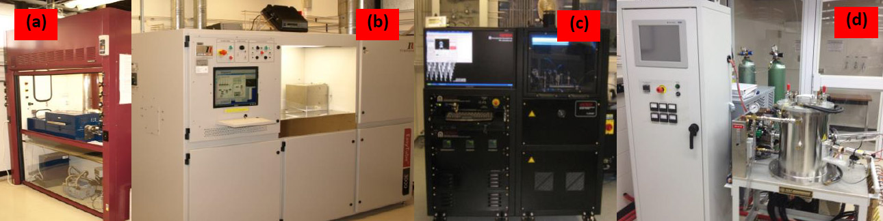
Figure 1. Manufacturing CNT arrays using Nanofurnaces: (a) First Nano ET1000 first generation reactor operational in 2002, can produce one 2.5x5 cm wafer in each experiment; (b) First Nano ET3000 second generation reactor, operational in 2007 and can produce one 10 cm wafer in two pieces in each experiment; (c) Black Magic Furnace by Aixtron, operational June 2013, can procduce one full 4 inch wafer per experiment with fast heating and cooling; (d) MRF annealing furnace 2,800°C.
Instrumentation in Nanoworld for Nanoscale Materials Processing:
- The nanoworld lab has vacuum processing glove boxes, ovens, balances, molds/nanocomposites.
- Spin Coater “Chemat” used in substrate preparation; Centrifuge “Fisher”.
- A Silverson mixer, a Fisher ultrasonicator probe, heater, RLC meter.
- Custom built machines for spinning carbon nanotube arrays into threads, Fig. 2(a).
- Custom built machines for drawing CNT sheet from arrays, Fig. 2(b).
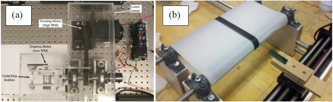
Figure 2. Spinning machine to produce CNT thread and yarn and Machine for drawing CNT sheet.
Instrumentation in Nanoworld Characterize CNT Materials and CNT-based Devices:
- A four-robot nanomanipulator made by Kleindiek to manipulate and handle nanosize objects, characterizing CNT and providing feedback. Fig. 3 shows the robots. Fig. 4 shows use of two robots.
- Instron Micro Testing Machine Model 5948 w/pneumatic grippers and resolution of mN- Fig. 5(a);
- Four probe instrument Jander Engineering Unit RM 3000/MHP 10-Fig.5(b).
- Environmental Scanning Electron Microscope XL30 FEG (D1531), Kleindiek Nanomanipulator.
- Signal processing instrumentation for characterizing CNTs; LeCroy (2), Textronics oscilloscopes, function gen. (3), multimeters (3), TREK amplifiers (2), power supplies, LABVIEW boards.
- Custom built electrochemistry analysis test bed including a Gamry Potentiostat (Model: PCI4/750) coupled with the EIS software (Gamry, EIS300), LABVIEW VI controller.
- MTS machine 15KN for testing nanocomposite samples, fiber testing machine, 4-point probe.
- Electronics instrumentation including: Electrochemical test systems, oscilloscopes etc.
- Custom-built fluidic system to measure the electrical impedance nanotube electrodes.
- Full access to UC Clean Room for microfabrication, E-beam deposition/lithography, ICP, lithography.
- Agilent vector network analyzer AT-N5222A, from 10 Hz to 26.5 GHz when analyzing CNTs.
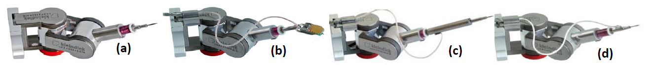
Figure 3. Plug-in tools to make submicron CNT thread. Micromanipulator with: (a) normal probe; (b) force measurement system; (c) rotational tip; (d) low current measurement kit. The four arm robot nanomanipulator made by Kleindiek can manipulate nanosize objects including CNT. This manipulator system is critical for characterizing CNT fibers and providing feedback to the synthesis and modeling.
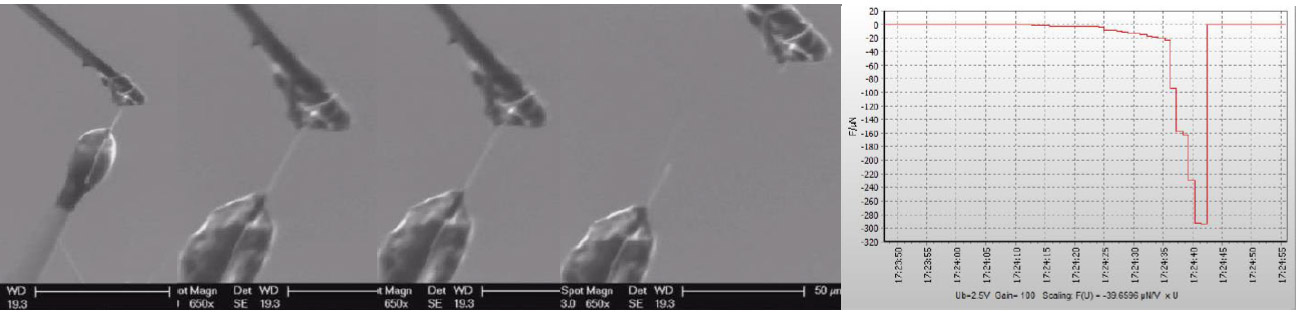
Figure 4. Kleindiek manipulator testing CNT fiber in a SEM, force versus time is measured.
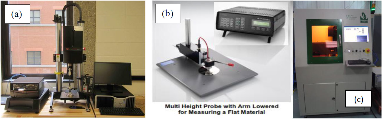
Figure 5. Test and machining equipment; (a) Instron Micro Testing Machine Model 5948 with resolution of mN; (b) Four probe instrument Jander Engineering Unit RM 3000/MHP; (c) Laser machining system.
CNT Materials Synthesis and Post Processing at UC.
The research facility processes nanoscale raw materials. Nanotube and nanowire materials and their post-processing come from the Nanoworld Lab, which is a college facility at UC. Magnetic nanomaterials are available commercially and we purchase and use them. Manufacturing and post-treatment of raw materials based on carbon nanotubes (CNT) and metal nanowires is directed by Vesselin Shanov. The Nanoworld Laboratory at UC has a good international reputation related to synthesis of unique nanostructured materials and nanocomposite materials. The properties of these materials are being improved by thermal treatment, densification, plasma treatment, doping and coating. Different approaches of post treatment that will be applied to the nanostructured raw materials and the related facilities designed, manufactured or acquired at UC available for this project.
Composites Manufacturing. Nanoworld is a one-stop shop for fabricating nanocomposties, Figure 6. All the equipment needed is already available. Two larger size Instron tensile tesing machines are also used.
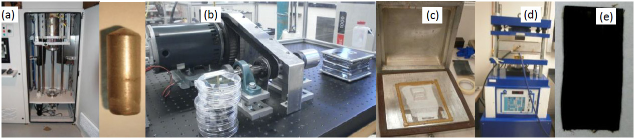
Figure 6. Nanoworld one-stop shop for fabricating materials: (a) Mg single crystal inch long; (b) spinning thread; (c) bag mold layup; (d) material curing in hot press; (e) IM7 977-3 embedded with CNT thread.
The UC Advanced Materials Characterization Center state-of-the-art analytical tools available are:
- Philips X’Pert MPD powder diffractometer system with associated hardware/software/peripherals.
- X”Pert PRO X-Ray diffraction system for thin film analysis.
- Hitachi S-4000 FEG Scanning Electron Microscope with Link ISIS Pentaflet thin-window detector
- Philips XL-30 FEG Environmental Scanning Electron Microscope with backscattered detector
- Philips CM20 200 kV Transmission Electron Microscope with EDAX NX-2 Ultra-thin window
- AFM Dimension 3100 Scanning Probe Microscope from Digital Instrument
- X-ray Photoelectron Spectrometer (XPS), Perkin-Elmer model 5300 Spectrometer
- Secondary Ion Mass Spectrometry Ion TOF SIMS IV Cameca, with 3 lens Ga gun, Ar gun
- A Nanonex NX-2600 Nanoimprint Lithography (NIL) System in the clean room.
Nanoworld also collaborates with different industries and government labs have additional facilities available for use on a limited basis. This instrumentation includes a Temescal e-beam machine for substrate preparation, ET-3000 EXT extended CVD nanofurnace for scale up of nanotube manufacturing, electrical characterization equipment for RF analysis, and HT oven for annealing CNT.
